Skip to content

The Banerjee Lab

Atomic-scale processes for materials discovery

  • Home
  • Publications
  • Research
  • Equipment
  • Teaching
  • People
  • Current Page: News
  • Home
  • Publications
  • Research
  • Equipment
  • Teaching
  • People
  • Current Page: News
The Banerjee Lab

News

banerjeelab_ucf

the banerjeelab@ucf develops new nanomaterials for energy applications at the University of Central Florida, Orlando

How are #SILICONCHIPS made? We are developing virt How are #SILICONCHIPS made? We are developing virtual lab modules to help students understand unit processes in #semiconductor manufacturing in EMA 4411 at #UCF #CECSUCF #MSEUCF. This one shows ion implantation in silicon, source / drain implant through a mask and post implant anneal.
How are #SILICONCHIPS made? We are developing virt How are #SILICONCHIPS made? We are developing virtual lab modules to help students understand unit processes in #semiconductor manufacturing in EMA 4411 at #UCF #CECSUCF #MSEUCF. This wet etch module shows the isotropic etching of SiO2 using a buffered oxide etchant and the Si etching using hot KOH.
How are #SILICONCHIPS made? We are developing virt How are #SILICONCHIPS made? We are developing virtual lab modules to help students understand unit processes in #semiconductor manufacturing in EMA 4411 at #UCF #CECSUCF #MSEUCF. This lithography module shows a photoresist contrast curve and the optical system combining to print patterns at the micro and nanoscale.
How are #SILICONCHIPS made? We are developing virt How are #SILICONCHIPS made? We are developing virtual lab modules to help students understand unit processes in #semiconductor manufacturing in EMA 4411 at #UCF #CECSUCF #MSEUCF. This one shows SiO2 growth inside trenches with and without a nitride mask.
How are #SILICONCHIPS made? We are developing virt How are #SILICONCHIPS made? We are developing virtual lab modules to help students understand unit processes in #semiconductor manufacturing in EMA 4411 at #UCF #CECSUCF #MSEUCF. This one shows how #Czochralski's growth and float zone refinement in action.
Group members @probablynottj and @maahir_rahi rep Group members @probablynottj  and @maahir_rahi represented our #NSFPREM center (http://prem2.cecs.ucf.edu) at the CAMPS2026 Conference (https://camps2026.engin.umich.edu/) at the University of Michigan this year with two wonderful posters on Atomic Layer Deposition (#ALD) of quantum materials. Great Job!!! 👏
We hosted some of the foremost groups in #atomicla We hosted some of the foremost groups in #atomiclayerdeposition #ald at #universityofcentralflorida earlier this month. Professors Kessells, Mackus from #tueindhoven and Professors Devi and Parala from #ifwdresden and their students/postdocs spent time in our ALD Labs. Thanks you!
An incredible wrap up for ALD/ALE 2026! It was an An incredible wrap up for ALD/ALE 2026! It was an honor to chair this amazing Conference. 350+ abstracts, 750+ attendees and meeting new and old friends! Thank you all for attending and see you all in Dresden next year!
Thank you #jawoollam for your 3-day #spectroscopic Thank you #jawoollam for your 3-day #spectroscopicellipsometry workshop at #ucf.
Our review article on carrier-selective and passiv Our review article on carrier-selective and passivating contacts for silicon PVs is out in Applied Physics Reviews. Its a round up of 300+ articles in this rapidly evolving field with recommendations on device standardization and predictions on future trends. Read all about it: “Atomic layer deposition (ALD) of passivating, carrier-selective oxides for silicon photovoltaics” Appl. Phys. Rev. 1 December 2025; 12 (4): 041330. https://doi.org/10.1063/5.0275420
Thanks @nicholasguinto from @Velian lab at UW for Thanks @nicholasguinto from @Velian lab at UW for visiting @jurcalab and @banerjeelab_ucf Labs at UCF and learning about our research. Hopefully we will extend this relationship to a great collaboration in the future. Thanks to the support from PREM funding!
Our class visit from EMA4411 - Principles of Semic Our class visit from EMA4411 - Principles of Semiconductor Manufacturing get a chance to enter the CECS cleanroom. Thanks to @ucfcecs cleanroom staff, @avrakundu and all ti, lmco and northrup grumman cleanroom fellows.
Our paper on super stable resistivity materials is Our paper on super stable resistivity materials is out in #advancedmaterials Thanks to all our collaborators.
https://advanced.onlinelibrary.wiley.com/doi/10.1002/adma.202514483
Our JANIS ST500 system allows us to test electroni Our JANIS ST500 system allows us to test electronic chips in a superbly controlled environment. Here we are testing a chip’s ability to respond visible photon by generating electrons at room temperature. # photocurrent #probestation
Great AVS71 with @probablynottj @bissell.eric @aye Great AVS71 with @probablynottj @bissell.eric @ayelencarolina  in Charlotte Sept 21-26 2025! Both @probablynottj  and @bissell.eric  presented great talks of their work. @ayelencarolina had her first poster at AVS and hopefully many to follow. Good times with old friends and new! We cant wait for AVS72 in Pitt!!!
Its the Gathering! Happy MAGICAL Friday!!!! #magic Its the Gathering! Happy MAGICAL Friday!!!! #magicthegathering
#atomiclayerdeposition #rotaryreactor #powderald @ #atomiclayerdeposition #rotaryreactor #powderald @bissell.eric coating 300 m^2 nanoparticles with atomic layer precision. @ucfresearch @ucfgradstudies @ucfcecs @ucfnanoclub
First videos on nanoparticle behavior simulated in First videos on nanoparticle behavior simulated in our powder ALD model reactors. Thanks to @bissell.eric wonderful creations to push the technology on #atomiclayerdeposition #powderALD Inspired by @ruudvanommen at #tudelft
@UCF Prem Center on quantum materials had a great @UCF Prem Center on quantum materials had a great time at UWs @MEMC MRSEC annual retreat in PackForest near the scenic Mt Rainier! Great science, great discussions and so much to look forward to. Thanks to @memc for organizing this productive retreat.
@bissell.eric latest paper on use of #atomiclayerd @bissell.eric latest paper on use of #atomiclayerdeposition (ALD) to restrict grain grown in nanocrystalline ceramics is out! This showcases our Lab's critical ability to coat high surface area nanoparticles with atomic layer precision. Congrats to all involved. 
https://pubs.acs.org/doi/10.1021/acsanm.5c02343
Follow on Instagram

Latest publications:

  • Near-zero temperature coefficient of resistivity, Adv Mater, 2025
  • Atomic layer deposition (ALD) of passivating, carrier-selective oxides for silicon photovoltaics
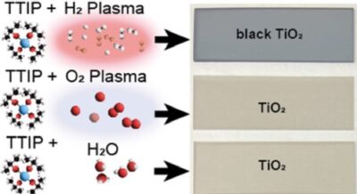
  • Black titania, Chem Mater 2024
    PEALD black TiO2
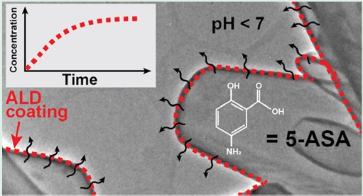
  • Controlled drug delivery with ALD "shells"
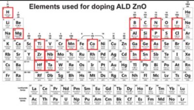
  • Review article ALD doped ZnO
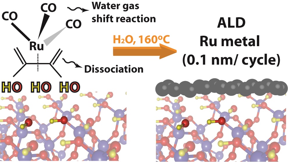
  • Ru metal ALD
  • Sub 2nm ALD Ru films

Address:

4353 Scorpius Drive, Research I Building
Orlando, FL 32816 – 0120, USA
Email Us

Follow us on Instagram

Recent Comments

    Translate

    The Banerjee Lab

    The Banerjee Lab © 2026. All Rights Reserved.

    Powered by WordPress. Theme by Alx.