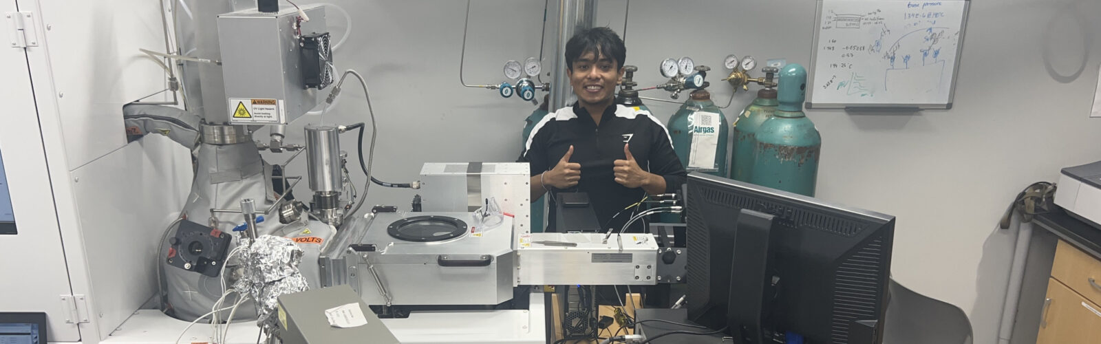
An undergraduate’s passion for studying materials at a nanoscopic level has earned him a monumental opportunity to pursue research for the U.S. Department of Energy (DOE).
Materials science student Maahir Rahi was selected to conduct research this summer in New York for the Experiential Learning Explorations in Advanced Nanomanufacturing program, or ELEAN, offered by Stony Brook University in collaboration with the DOE’s Brookhaven National Laboratory.
A Jacksonville native, Rahi was inspired to pursue engineering by his grandfather, a civil engineer who studied at Bangladesh University of Engineering and Technology. The decision to study materials science was just a logical choice initially, a field that checked the boxes because it combined Rahi’s interests in chemistry, math and physics. His passion for the field grew steadily as he learned more about the discipline in the Banerjee Lab, directed by Professor Parag Banerjee.
“What I didn’t anticipate was how much I would enjoy the way materials science encourages you to understand systems at a deeper level through the fundamental structure-property-processing relationships that govern material behavior, a concept my PI, Dr. Banerjee, emphasized during our very first meeting and one that has stayed with me ever since,” he says.
His studies align perfectly with his love of computers, which started when he was a child. Always one to build computers to understand how they worked, his fascination with semiconductors has stayed with him and now features in his research, allowing him to examine computing at the atomic level.
“Understanding and developing those materials is what excites me most about the field, because it means the opportunity to work towards enabling the future of computing,” he says.
Optimizing Atomic Structures for Future Technologies
In the lab, Rahi helps develop novel materials for future electronic and energy technologies using atomic layer disposition (ALD) and atomic layer etching (ALE), work he says is already widely used in real-world applications from semiconductor manufacturing to energy applications.
One pivotal experience that reinforced his passion for the field took place in the lab. He was measuring the resistance of a silicon substrate coated with a nanometer thin film as compared to an otherwise identical sample that had not been coated, and was astonished at the outcome.
“What amazed me was that the two samples looked completely identical to the naked eye. The only difference was an incredibly thin layer of deposited material, yet that atomic-scale change transformed the electrical behavior of the surface by many orders of magnitude,” he says.
This summer at Brookhaven National Lab, he has the opportunity to cultivate his passion for materials science even further. He says his focus at the REU is on fabricating metal oxides semiconductor field effect transistor (MOFSET) devices, using metal oxide semiconductor materials with amorphous and nanocrystalline phase compositions.
“The goal is to study whether these material systems can produce useful or potentially novel electronic properties, which could contribute to future semiconductor device research or implementation into the semiconductor manufacturing industry,” he says.
Advocating for Materials Science at UCF
He’s committed to his field outside the lab as well. Rahi is the president of the UCF chapter of Material Advantage, an organization that offers opportunities and camaraderie for materials engineering students. He also a co-founder and vice president of the Semiconductor Career Readiness Organization, serves on the Materials Science and Engineering Student Advisory Council, and attends IEEE events.
Rahi is grateful to his advisor, Parag Banerjee, his mentor Terrick McNealry James, the University of Central Florida and University of Washington Partnership for Research and Education in Materials (PREM) and the UCF material science community for their mentorship and support.
“I hope my story can help highlight the department’s continued success in preparing undergraduates for advanced research in materials science through areas such as semiconductors and nanoscience.”
- Written by Bel Huston